
What is a shift register? When should we use it?
A shift register is an Integrated Circuit (IC), which allows us to expand the number of pins we can use on our Arduino Board (in fact, any micro-controller).
So far we learned about many different components and sensors like an LED, buzzer, RGB LED, DHT11 sensor, potentiameter, photoresistor, and an Ultrasonic Sensor. What if we want to put all these components and many more, for some big project? Soon we will run out of pins on the Arduino board. This is when a shift register comes in use. The shift register will expand the number of pins on our board. Even if we run out of pins after using the shift register, we can use multiple shift registers and chain them.
How does the 74HC595 Shift Register work?
The 74HC595 shift register gives us 8 output pins. The 74HC595 shift register is connected to the Arduino board using 3 pins. One for the data, one for the clock, and one for the latch.
Using the data and clock pin, we insert data into the shift register serially. We can insert 8 bit of data at a time using the shiftOut function. When we insert 8 bit of data through the data pin, it travels serially and moves through each output pin and eventually all output pins get data. That means, first bit of data, which is supposed to go to the last output pin, travels from the first pin to the next, and finally reaches its destination output pin. That means if we have connected LEDs (or any component) to our output pins, it will flicker as soon as it recives its HIGH or LOW value. To prevent that, the latch pin comes in handy.
So when the latch pin is LOW (off), all the data that we sent will be stored into the storage register (clock) and will not be available to the output pins, util we set the latch pin to HIGH (on). This will prevents the flickering, as we mentioned in the paragraph above.
The pin number 13 is output enabled (OE) pin. It works as the negative switch, which means when it is LOW, the shift register in on, and when it is HIGH, the shift register in off.
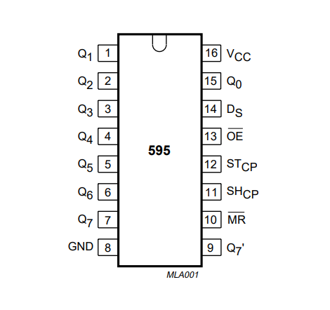
The image above shows the schematic of the 74HC595 shift register.
- Pins Q0 to Q7 are all output pins
- The GND is for the ground
- The Vcc is for the power
- The DS is for the data pin
- The OE is the output Enable pin
- The STCP is the latch pin (storage register)
- The SHCP is the clock pin (shift register)
- The MR is the master reset pin
- The Q7 is the serial data output
Let’s use the Shift Register and build a circuit to make the LEDs blink in a pattern
Components needed
- 8 leds
- 8 resistors
- Jumper cables
- Capacitor
- Shift Register (74HC595)
- 2 breadboards
- Arduino Uno Board
- A computer with an Arduino IDE installed
Completed Circuit


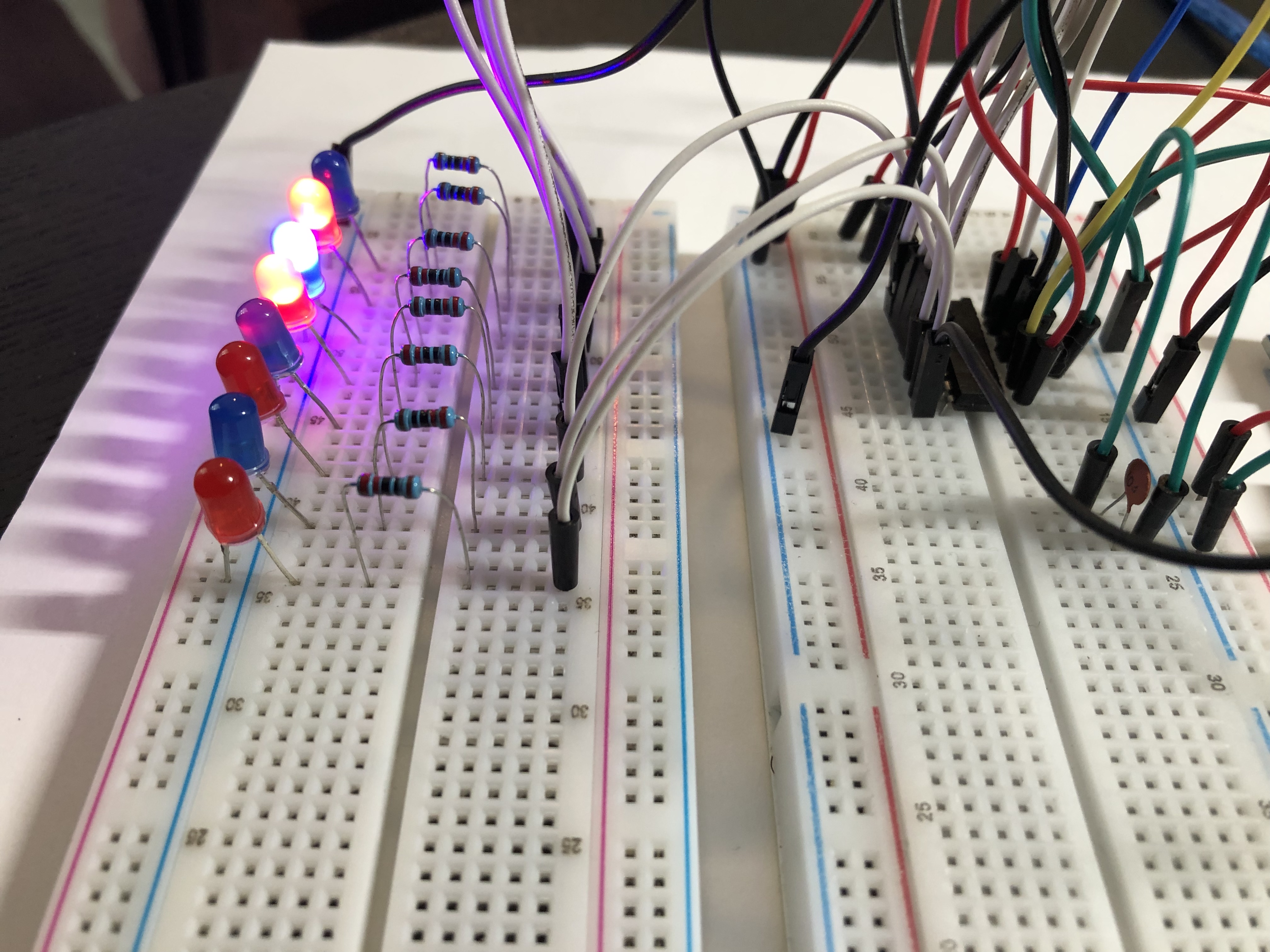
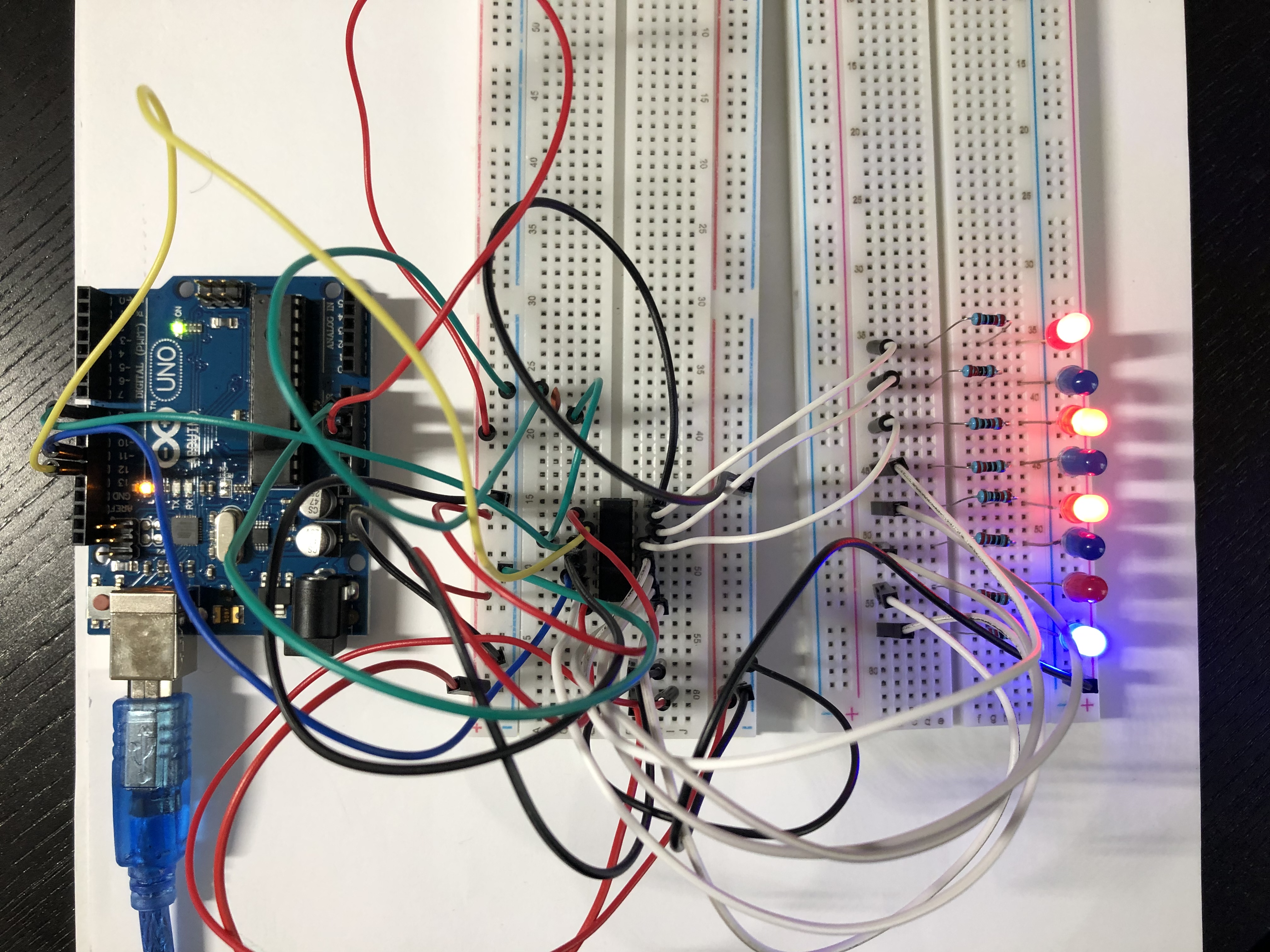

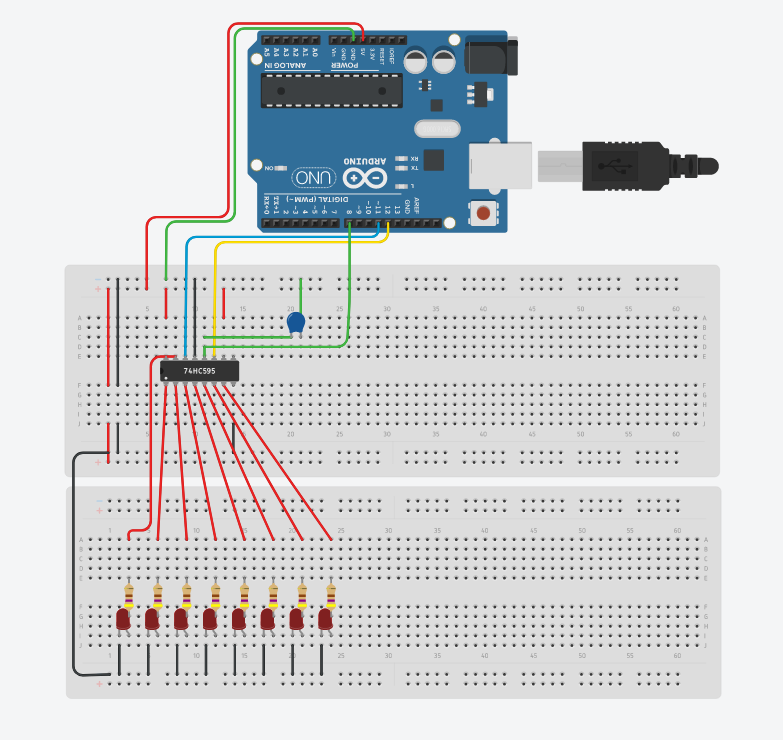
The image above is completed circuit showing the use of shift register. First put the shift register on the breadboard. Now we will connect all the pins of the shift register.
First connect the shift register to the Arduino board. As discussed earlier, we need to connect the three pins of the shift register (data pin, latch pin and the clock pin) to digital pin number 11, 8 and 12 on the Arduino board. Now connect the power pin (pin 16 of shift register) and GND pin (pin 8 of shift register) to the power and ground.
Now the shift register is connected to Arduino board and ready to use. We got new 8 output pins on the shift register. As shown in the image above, we have connected 8 leds to all 8 output pins of shift register. Please connect first led to Q0 pin of the shift register, second led to Q1 pin of the shift register and so on for all 8 leds so we can easily make the leds blink in pattern.
The program
//Pin connected to ST_CP of 74HC595
int latchPin = 8;
//Pin connected to SH_CP of 74HC595
int clockPin = 12;
////Pin connected to DS of 74HC595
int dataPin = 11;


byte leds1 = 0b10101010;
byte leds2 = 0b01010101;

byte ledF1 = 0b10000001;
byte ledF2 = 0b01000010;
byte ledF3 = 0b00100100;
byte ledF4 = 0b00011000;

byte ledUp0 = 0b00000000;
byte ledUp1 = 0b10000000;
byte ledUp2 = 0b11000000;
byte ledUp3 = 0b11100000;
byte ledUp4 = 0b11110000;
byte ledUp5 = 0b11111000;
byte ledUp6 = 0b11111100;
byte ledUp7 = 0b11111110;
byte ledUp8 = 0b11111111;

void setup()
{
  pinMode(latchPin, OUTPUT);
  pinMode(dataPin, OUTPUT);
  pinMode(clockPin, OUTPUT);
}

void loop()
{

  // binaryNumberDisplay();
  ledPattern();
  //pingPong();
  //backAndForth();

}

void backAndForth()
{
  pushData(200, ledUp0);
  pushData(200, ledUp1);
  pushData(200, ledUp2);
  pushData(200, ledUp3);
  pushData(200, ledUp4);
  pushData(200, ledUp5);
  pushData(200, ledUp6);
  pushData(200, ledUp7);
  pushData(200, ledUp8);
  pushData(200, ledUp7);
  pushData(200, ledUp6);
  pushData(200, ledUp5);
  pushData(200, ledUp4);
  pushData(200, ledUp3);
  pushData(200, ledUp2);
  pushData(200, ledUp1);
  pushData(200, ledUp0);
}

void pingPong()
{
  int delayTime = 200;
  pushData(delayTime, ledF1);
  pushData(delayTime, ledF2);
  pushData(delayTime, ledF3);
  pushData(delayTime, ledF4);
  pushData(delayTime, ledF3);
  pushData(delayTime, ledF2);
}


void ledPattern()
{
  pushData(200, leds1);
  pushData(200, leds2);
}

void binaryNumberDisplay()
{
  for (int leds5 = 1; leds5 < 255; leds5++)
  {
    pushData(500, leds5);
  }
}

void pushData(int delayTime, byte data)
{
  delay(delayTime);
  digitalWrite(latchPin, LOW);
  shiftOut(dataPin, clockPin, LSBFIRST, data);
  digitalWrite(latchPin, HIGH);
}
As we mentioned earlier, 74HC595 shift register is SIPO which means Serial In Parallel Out. We give data to the shift register via Data pin along with Clock pin. To do that we will use shiftOut function.
The shiftOut function takes 4 parameters as shown below.
shiftOut(dataPin, clockPin, bitOrder, value)
First parameter is the dataPin and second parameter is the clockPin. The third parameter is for bit order. We can set it to MSBFIRST (Most Significant Bit First) or LSBFIRST (Least Significant Bit First). The fourth parameter and the most important parameter is the value (data). The allowed type of for value is byte (8 bits for 8 output pins).
For example, if we give value of byte 10000000 with bit order MSBFIRST, the first pin will get HIGH voltage and rest seven pins will get LOW voltage. In our circuit above, this will make first LED on and rest of the LEDs off.
Notice that we are first setting the latchPin to LOW (off) and then shifting our data in and then setting the latchPin back to HIGH (on). As mentioned earlier, if we don’t do that, our LEDs will flicker as data moves through different pins during input. When latch pin is off, all input bits are stored in storage register and when latch pin is on, all stored bits will be shifted out.
Please watch the video below for explanation of circuit and the program.

One thought on “74HC595 Shift Register”